What are charge-coupled devices (CCDs) and why are they so important in astrophotography
When you take a picture with your cell phone or a digital camera, you rarely think about what's going on inside. However, whether we're examining distant galaxies, fluorescent cells, or atomic structures, precision and sensitivity are crucial.
May 21, 2025
When you take a picture with your cell phone or a digital camera, you rarely think about what's going on inside. However, whether we're examining distant galaxies, fluorescent cells, or atomic structures, precision and sensitivity are crucial.
This is where CCDs come in: charge-coupled devices that have revolutionized the way we capture and analyze light.
But how can a simple chip convert photons into digital data? Today, we will explain it to you in step-by-step detail.
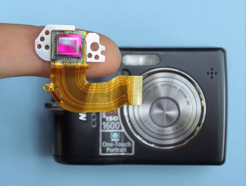
CCDs are image sensors based on the displacement of electrical charges generated by the light that falls on them. They offer very high image quality and sensitivity, albeit at the cost of higher energy consumption and manufacturing costs compared to other technologies, such as CMOS.
Its use remains key in scientific and professional applications where optimal performance is crucial for achieving good results in images and/or photographs.
Working principle of CCDs
Imagine a sensor that not only detects light but also converts it into a stream of electrons that is then translated into a digital image. This is how a CCD, or charge-coupled device, works - a key technology in astronomy, medicine, and advanced science.
Its operation begins at the microscopic level, in each pixel of the sensor. A CCD is composed of an array of tiny cells called "potential wells," each equivalent to one pixel in the final image. Each well is designed to capture photons, i.e., particles of light, during exposure time.
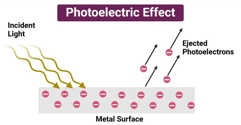
When a photon enters one of these wells, it releases an electron through the photoelectric effect. Albert Einstein initially described this phenomenon, and it is the same principle that explains how light can generate electricity.
In the CCD, each photon that strikes releases an electron, and the number of electrons accumulated in each pixel is directly proportional to the intensity of the light that reached it. Thus, a brighter area will generate more electrons than a darker one.
So far, the CCD has converted light into an electrical charge. But how does that transform into an image? This is where the genius of "coupled scrolling" comes in.
After exposure is complete, the charges stored in each pixel are not read directly in place, but instead moved in a chain, row by row, to an edge of the chip.
It is like a row of buckets full of water that are poured into each other until they reach the last one. The latter "cuvette" is connected to an amplifier, which converts the accumulated electrical charge into a voltage.
That voltage, in turn, is digitized by an analog-to-digital converter, transforming the information in each pixel into digital numbers that, when processed, build an image.
This process is exact, as it can count individual electrons, allowing it to detect very low levels of light, which is ideal for astronomy or fluorescence microscopy.
However, it is also a sequential process, which means that the reading speed is limited by the need to transfer electrons, pixel by pixel, until the entire image is complete.
Basic structure of a CCD
Although the workings of CCDs seem almost magical, their structure is the result of meticulous engineering and deeply understood physics.
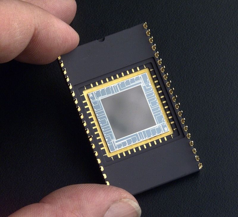
At first glance, a CCD is a small rectangular chip that could be mistaken for any other integrated circuit. But inside, there is a perfectly organized array of pixels, each designed to capture and store light with extraordinary sensitivity.
The structure of a CCD is based on a semiconductor, usually silicon, on which millions of tiny cells called potential wells are created. These wells are nothing more than small regions where electrical charge can be stored. The key is in how these wells are formed and how they are manipulated.
Each pixel is covered by one or more metal oxide electrodes, usually polysilicon, which overlap slightly with each other. These electrodes are connected to an electronically controlled voltage source.
By applying a sequence of specific voltages, engineers can create a "tilt" in the chip's electric field, as if it were a descending hill for electrons. This tilt allows the load to move from one pixel to the next, in a kind of microscopic "conveyor belt."
But there is more. Each pixel acts like a small capacitor: when light hits the silicon and generates electrons, they are trapped in the corresponding potential well.
The structure of the CCD prevents electrons from escaping until the transfer sequence is applied. And it's this ability to hold the charge during exposure and then move it in a block that gives the device its name: "coupled charge."
Once the light has been collected, the loads stored in each row are transferred vertically downwards until they reach a special row: the displacement register.
This register is an additional horizontal row that acts as a fast output channel. There, each pixel in the row is transferred, one by one, to a readout amplifier located on one of the edges of the chip.
This amplifier is a critical component; it converts the accumulated charge in each pixel into a voltage signal, which is then digitized. It's essential to note that this entire process is sequential: only one pixel is read at a time, which limits the maximum reading speed but allows for unparalleled uniformity and accuracy.
CCD Modes of Operation
The basic architecture of a CCD is remarkably efficient. Still, its true versatility lies in the different modes of operation that allow the sensor to be adapted to different technical needs.
These modes determine how the image is captured and transferred within the chip, and each has particular advantages and limitations that make it ideal for specific applications.
There are three main modes: full-frame, frame-transfer, and interline transfer. Understanding them is essential to appreciate how CCDs have become indispensable tools in fields such as astronomy and biomedicine.
1. Full-frame
Let's start with the full-frame mode, the simplest from a structural standpoint. In this mode, the entire chip surface is dedicated to capturing light, enabling maximum detection efficiency.
Each pixel in the array is an active detector, with no additional structures interfering with photon capture. However, as the entire chip is exposed to light during the acquisition process, it is imperative to use an external mechanical shutter that blocks light from entering while the image is being read.
Otherwise, the light would continue to generate charge while the data is being transferred, producing distortions and noise known as "smearing." This mode is used when sensitivity is the priority and exposure conditions can be perfectly controlled, such as in astronomical research telescopes.
2. Frame-transfer
The second mode is frame-transfer, a clever solution to the read-time problem. Here, the matrix of the CCD is divided into two identical halves. The upper half is used to capture the image, while the lower half acts as a "storage zone" protected from light.
Once the exposure is complete, the entire image is quickly transferred from the capture area to the storage area. This happens in a fraction of a second, allowing for a slower reading and eliminating the risk of the image being contaminated by new light.
This design eliminates the need for a mechanical shutter, albeit at the cost of doubling the chip's size and reducing spatial efficiency.
3. Interline transfer
Finally, we have the interline transfer mode, perhaps the most sophisticated and versatile of the three. In this design, each column of photodetector pixels has an equivalent column of storage pixels adjacent to it, covered with an opaque shield that blocks light. When the exposure is over, the charge is transferred laterally, in microseconds, to the adjacent storage area.
From there, it is read sequentially without interference. This system enables images to be scanned, eliminating the need for an external shutter and resulting in virtually zero load drag.
However, because a portion of the chip area is occupied by storage pixels, the light detection efficiency per surface decreases unless microlenses are used to redirect the light to the active pixels.
Each of these modes responds to different needs: full-frame is ideal for maximum sensitivity in controlled conditions; frame-transfer is useful when speed is required without compromising quality, and Interline Transfer dominates in high-speed scientific and video cameras, where the immediacy of capture and the absence of artifacts are crucial.
Advantages and disadvantages of CCDs compared to other technologies
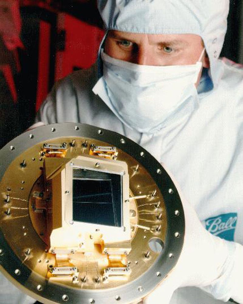
Since their invention in 1969, CCDs have been recognized as one of the most revolutionary technologies for image capture. Their ability to transform light into digital data with extraordinary fidelity quickly made them the gold standard in scientific applications.
But like any technology, CCDs have both notable strengths and significant limitations, especially when compared to their newer competitors, such as CMOS sensors.
Among its main advantages, its very high sensitivity to light stands out. A well-designed CCD can detect even a few individual photons per pixel, making it an irreplaceable tool for observing extremely faint objects, such as distant galaxies or faint fluorescence in biological samples.
This sensitivity is due to its excellent quantum efficiency, which in some models exceeds 90%, which means that more than 90% of the photons that hit the chip are converted into useful electrons.
In addition, CCDs have extremely low read noise. Thanks to its sequential readout architecture, where each pixel is transferred to the same amplifier, the noise level is very uniform and predictable.
This makes them ideal for measuring minimal differences in intensity, such as in spectroscopy or long-exposure astronomical imaging. This homogeneity also translates into another crucial advantage: excellent pixel-to-pixel uniformity.
Unlike CMOS sensors, which have each pixel with its readout circuit (and therefore exhibit slight variations in behavior), CCDs ensure that each pixel is virtually identical to the rest, greatly simplifying calibration and image processing.
However, these advantages come at a price, and this is where the disadvantages appear. The first and most apparent is high energy consumption.
CCDs require relatively high voltages and complex control electronics to manage charge transfer between pixels, resulting in increased energy use and the need for cooling systems to reduce thermal noise.
Another major limitation is the read speed, which is significantly lower than in CMOS sensors. Since CCDs read the image sequentially, pixel by pixel, any attempt to increase the resolution or capture frequency involves longer read times.
This makes them ill-suited for applications that require real-time video or ultra-fast capture, such as in certain branches of robotics or machine vision.
There's also the cost of manufacturing, which is generally higher than that of CMOS sensors. Manufacturing a CCD requires more delicate and controlled processes, and its performance also decreases rapidly with manufacturing defects or impurities.
This means that only specialized manufacturers can produce scientific-grade CCDs, which restricts their availability and raises prices.
Despite these disadvantages, CCDs remain the preferred choice when maximum accuracy, sensitivity, and uniformity are required. They are especially valued in scientific applications such as astronomy, where the quality of the scientific image cannot be compromised, even if it means sacrificing speed or energy efficiency.
Main applications of CCDs
While DCCs were born as a technological curiosity in the late 1960s, their impact on modern science and technology has been profound and long-lasting.
These sensors have found their place in some of humanity's most precise and sophisticated instruments, extending our vision beyond the limits of the human eye.
Their accuracy, sensitivity, and reliability have made them indispensable in fields where seeing more and seeing better is not an option, but a necessity.
One of the fields where CCDs have left an indelible mark is astronomy. We could say that the revolution of modern astrophotography would not have been possible without them.
Before their arrival, astronomers relied on chemical photographic plates, which were insensitive, unwieldy, and of low resolution. The introduction of CCDs increased the sensitivity of telescopes by more than 100 times, making it possible to detect galaxies millions of times fainter than those that could be seen previously.
Today, telescopes such as Hubble, Subaru, or those at the Paranal Observatory in Chile utilize advanced CCDs to capture images of the deep universe, spectra of stars, and cosmic structures with unprecedented clarity.
But its usefulness is not limited to outer space. In fluorescence microscopy, CCDs are essential for observing cellular structures labeled with fluorescent compounds.
Thanks to their high sensitivity and low noise, they can detect extremely weak light emissions, which is crucial in biomedical research where the behavior of proteins, genes, or viruses within living cells needs to be observed. The temporal and spatial resolution they offer has enabled advances in cell biology, neuroscience, and drug development.
In the field of laboratory spectroscopy, CCDs act as detectors in systems that analyze the chemical composition of a sample through light. From identifying contaminants in water to studying organic compounds in medicine or quantum physics, CCDs allow the intensity of light at different wavelengths to be recorded with great precision. This is crucial for obtaining reliable results in environments where every photon matters.
They also play a crucial role in medical imaging, especially techniques that require extremely high resolution, such as positron emission tomography (PET) or certain forms of digital radiography.
In these applications, the CCD's ability to record subtle variations in light enables the generation of detailed images of the inside of the human body, facilitating more accurate and earlier diagnoses.
And, of course, we cannot overlook their role in the industry. In automated quality inspection, particularly in the manufacture of microchips, pharmaceuticals, or optical components, CCDs are used to detect microscopic defects of this size.
The uniformity and consistency of these sensors ensure that each pixel measures the same, which is critical when inspecting objects that must meet micron tolerances.
In short, CCDs aren't just light sensors; they are the electronic eyes of modern science. From observing galaxies billions of light-years away to studying a moving cell or inspecting a microscopic weld in a factory, these devices have transformed the way we interact with the world and the universe.
CCDs teach us that even the faintest light can be captured, understood, and transformed into knowledge. They are the silent bridge between the universe and our eyes, between the invisible and the observable.